32% SPACE Epitaxial Wafer
Details
OVERVIEW
——
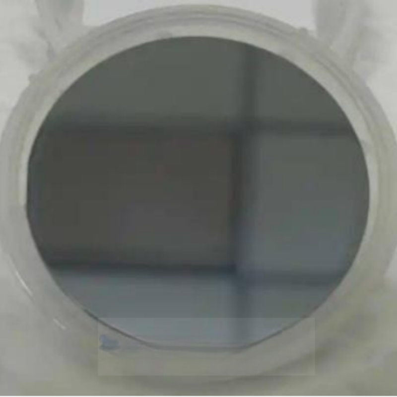
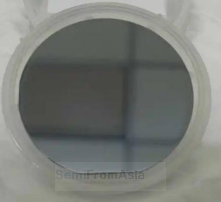
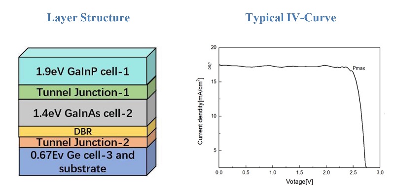
SPACE Wafers contain triple junction InGaP/GaAs/Ge epi-layer structures with efficiencies of up to 32% available in large-scale production.These SPACE wafers can be used for any further processing and customized cell designs.The unprocessed Epitaxial Wafers of class 32% contain our high- efficiency GaInP/GaAs/Ge based epitaxial layers on a Ge substrate. These epixial wafers can be used for any further processing and customized cell designs.
SPECIFICATIONS
——
Substrate Material :GaInP/GaInAs/Ge on Ge substrate Base
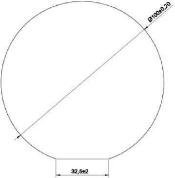
Material :100 mm ±0.20
Thickness :145 μm ±15 μm or 175 μm ±15 μm
Major Flat length :32.5 mm ±2 mm
Major Flat orientation:(100) ±2°
Average Weight :≤ 93 mg/cm2
Laser mark labelAlpha-numeric
Typical Performance Data
——

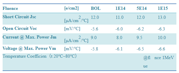
Temperature Gradients
——
Layer StructureTypical IV-Curve
——
FAQ
——
1. About Price:
All of our prices are competitive and negotiable. The price varies depending on the configuration and customization complexity of your device.
2. About Sample:
We can provide sample production services for you, but you may provide some fees.
3. About Payment:After the plan is confirmed, you need to pay us a deposit first, and the factory will start preparing the goods. After the
goods is ready and you pay the balance, we will ship it.
4. About Delivery:
After the goods manufacturing is completed, we will send you the acceptance video, and you can also come to the site to inspect the equipment.