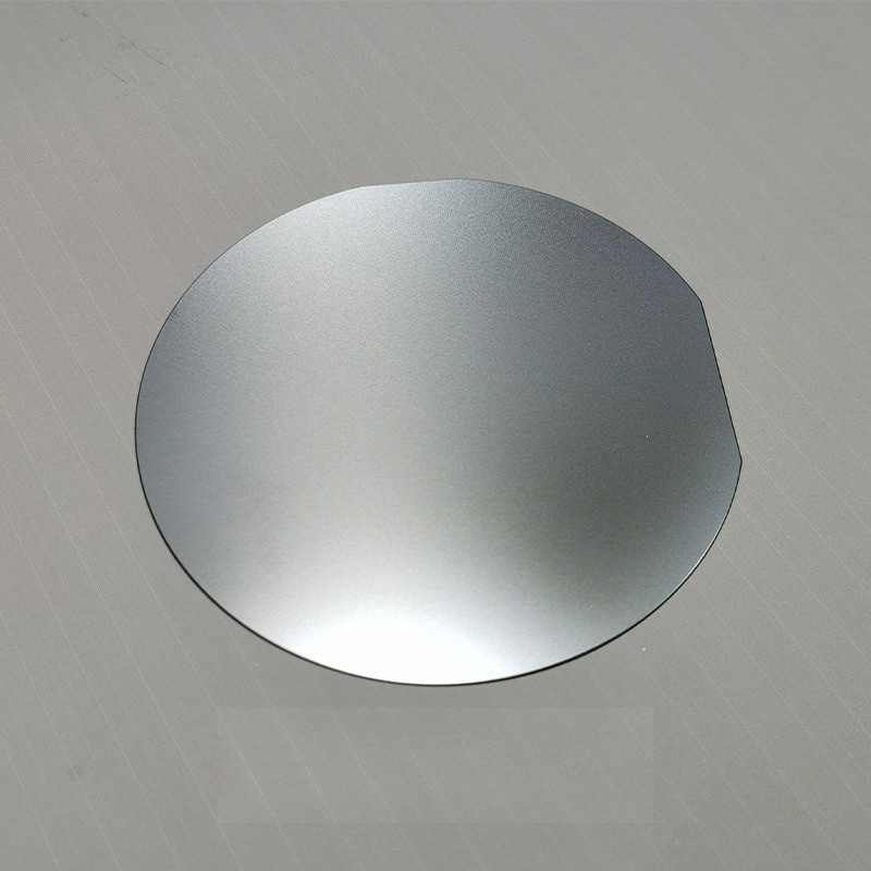
Gallium Arsenide GaAs substrate wafer
OVERVIEW
——
Gallium Arsenide GaAs substrate wafer is a direct band gap compound semiconductor of group III-V synthesized by at least 6N 7N high purity gallium and arsenic element, and grown crystal by VGF or LEC process from high purity polycrystalline gallium arsenide, grey color appearance, cubic crystals with zinc-blende structure. With the doping of carbon, silicon, tellurium or zinc to get n-type or p-type and semi-insulating conductivity respectively, a cylindrical InAs crystal can be sliced and fabricated into blank and wafer in as-cut, etched, polished or epi-ready for MBE or MOCVD epitaxial growth. Gallium Arsenide wafer is principally used to fabricate electronic devices such as infrared light-emitting diodes, laser diodes, optical windows, field-effect transistors FETs, linear of digital ICs and solar cells. GaAs components are useful in ultra-high radio frequencies and fast electronic switching application, weak-signal amplification applications. Furthermore, Gallium Arsenide substrate is a ideal material for the manufacture of RF components, microwave frequency and monolithic ICs, and LEDs devices in optical communications and control systems for its saturating hall mobility, high power and temperature stability.
SPECIFICATIONS
——
| No. | Items | Standard Specification | |||
| 1 | Size | 2" | 3" | 4" | 6" |
| 2 | Diameter mm | 50.8±0.3 | 76.2±0.3 | 100±0.5 | 150±0.5 |
| 3 | Growth Method | VGF | VGF | VGF | VGF |
| 4 | Conductivity Type | N-Type/Si or Te-doped, P-Type/Zn-doped, Semi-Insulating/Un-doped | |||
| 5 | Orientation | (100)±0.5° | (100)±0.5° | (100)±0.5° | (100)±0.5° |
| 6 | Thickness μm | 350±25 | 625±25 | 625±25 | 650±25 |
| 7 | Orientation Flat mm | 17±1 | 22±1 | 32±1 | Notch |
| 8 | Identification Flat mm | 7±1 | 12±1 | 18±1 | - |
| 9 | Resistivity Ω-cm | (1-9)E(-3) for p-type or n-type, (1-10)E8 for semi-insulating | |||
| 10 | Mobility cm2/v.s | 50-120 for p-type, (1-2.5)E3 for n-type, ≥4000 for semi-insulating | |||
| 11 | Carrier Concentration cm-3 | (5-50)E18 for p-type, (0.8-4)E18 for n-type | |||
| 12 | TTV μm max | 10 | 10 | 10 | 10 |
| 13 | Bow μm max | 30 | 30 | 30 | 30 |
| 14 | Warp μm max | 30 | 30 | 30 | 30 |
| 15 | EPD cm-2 | 5000 | 5000 | 5000 | 5000 |
| 16 | Surface Finish | P/E, P/P | P/E, P/P | P/E, P/P | P/E, P/P |
| 17 | Packing | Single wafer container sealed in aluminum composite bag. | |||
| 18 | Remarks | Mechanical grade GaAs wafer is also available upon request. |
Application
——
Gallium Arsenide GaAs wafers are principally used to fabricate electronic devices such as infrared light-emitting diodes, laser diodes, optical windows, field-effect transistors FETs, linear of digital ICs and solar cells. GaAs components are useful in ultra-high radio frequencies and fast electronic switching application, weak-signal amplification applications. Furthermore, Gallium Arsenide substrate is a ideal material for the manufacture of RF components, microwave frequency and monolithic ICs, and LEDs devices in optical communications and control systems for its saturating hall mobility, high power and temperature stability.
Delivery
——
Gallium Arsenide GaAs can be supplied as polycrystalline lump or single crystal wafer in as-cut, etched, polished, or epi-ready wafers in a size of 2” 3” 4” and 6” (50mm, 75mm, 100mm, 150mm) diameter, with p-type, n-type or semi-insulating conductivity, and <111> or <100> orientation. The customized specification is for the perfect solution to our customers worldwide.
FAQ
——
1. About Price:
All of our prices are competitive and negotiable. The price varies depending on the configuration and customization complexity of your device.
2. About Sample:
We can provide sample production services for you, but you may provide some fees.
3. About Payment:After the plan is confirmed, you need to pay us a deposit first, and the factory will start preparing the goods. After the
goods is ready and you pay the balance, we will ship it.
4. About Delivery:
After the goods manufacturing is completed, we will send you the acceptance video, and you can also come to the site to inspect the equipment.